This comprehensive guide provides an authoritative overview of buck converter design, covering fundamental concepts, key components, design considerations, and best practices. From understanding duty cycle and inductor ripple current to achieving output regulation, minimizing output ripple voltage, and optimizing transient response, this guide empowers engineers with the knowledge and techniques to design highly efficient and reliable buck converters.
Buck Converter Design Guide: Master the Art of DC-DC Conversion
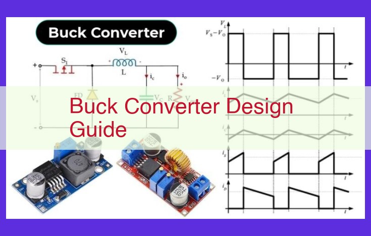
Buck converters are ubiquitous in electronic systems, providing a reliable and efficient means of converting DC power to a lower voltage. Designing these converters can be a daunting task, but with a clear understanding of their fundamental principles, you can navigate the process with confidence. Let’s embark on a journey to unravel the complexities of buck converter design.
Duty Cycle: The Heartbeat of the Converter
At the core of buck converter operation lies the concept of duty cycle. It represents the fraction of time during which the switching transistor is turned ON in relation to the entire switching period. This ON time, also known as on-time (t_ON), is inversely proportional to the switching frequency (f_SW) and output voltage (V_OUT).
The duty cycle (D) is defined as the ratio of t_ON to the total switching period (T_SW), expressed as:
D = t_ON / T_SW
Understanding duty cycle is crucial for controlling the converter’s output voltage. By adjusting the ON time of the switching transistor, you can regulate the output voltage to meet your system’s requirements. It’s like the conductor of an orchestra, coordinating the switching action to produce the desired output.
Buck Converter Design Guide
Chapter 1: Understanding Duty Cycle
The Importance of Duty Cycle
In the realm of buck converters, duty cycle reigns supreme. This critical parameter dictates how long the converter remains in its “on” state relative to its overall switching period. It directly influences the converter’s output voltage and current characteristics.
Relationship to Switching Period, On-Time, and Off-Time
The switching period is the time elapsed between two consecutive switching cycles. On-time refers to the duration during which the converter is in its conductive state, allowing current to flow. Off-time is the period when the converter is non-conductive.
The duty cycle (D) is mathematically expressed as:
D = On-Time / Switching Period
By varying the duty cycle, engineers can fine-tune the converter’s behavior to achieve desired output voltage and current levels.
Understanding Inductor Ripple Current: Its Impact and Significance
In the world of buck converters, inductor ripple current plays a crucial role in shaping the converter’s performance. Imagine a rollercoaster ride where the ups and downs represent the flow of current through the inductor. Just like an unpredictable rollercoaster, this ripple current can introduce noise and fluctuations into the converter’s output.
What’s Inductor Ripple Current?
Inductor ripple current is the fluctuating component of current that flows through the inductor during the switching period. It’s caused by the on-and-off nature of the switching action in the converter. When the switch is on, current flows through the inductor, building up magnetic energy. When the switch is off, the inductor releases this energy, causing the current to flow in the opposite direction.
Why Inductor Ripple Current Matters
High ripple current can lead to several undesirable effects in buck converters. Firstly, it can cause inductor core losses, which reduce the converter’s efficiency. Secondly, it can introduce noise into the output voltage, affecting the precision and performance of the connected devices. Additionally, excessive ripple current can cause saturation in the inductor, compromising its ability to store and release energy effectively.
Factors Influencing Ripple Current
The magnitude of inductor ripple current depends on several factors, including:
- Inductance (L): Higher inductance reduces ripple current.
- Switching frequency (f): Higher switching frequency increases ripple current.
- Output current (Iout): Higher output current increases ripple current.
- Duty cycle (D): Duty cycle also influences ripple current, but its effect is less pronounced than the other factors.
Factors influencing ripple current, including inductance, switching frequency, and output current
Calculating Inductor Ripple Current: Unveiling the Impact of Key Factors
Understanding the intricate dance between inductance, switching frequency, and output current is paramount when calculating inductor ripple current. This elusive current, a byproduct of buck converter operation, can significantly affect the overall performance and stability of the circuit.
Inductance: The Gatekeeper of Current Flow
Inductance, measured in henries (H), represents the magnetic energy stored in the inductor. It acts like a gatekeeper, resisting changes in current flow. The higher the inductance, the greater the opposition to current fluctuation. This means that a high inductance inductor will result in a smaller ripple current.
Switching Frequency: The Cadence of Power Transfer
The switching frequency, measured in kilohertz (kHz), determines how often the buck converter switches between on and off states. A higher switching frequency allows for a smaller ripple current because the inductor has less time to store magnetic energy during each switching cycle.
Output Current: The Load on the Converter
The output current, measured in amperes (A), represents the current demand from the load connected to the buck converter. A heavier load, demanding a higher output current, will draw more current from the inductor, leading to a larger ripple current.
Interplay of Factors: A Delicate Balancing Act
These three factors, inductance, switching frequency, and output current, dance in harmony to shape the ripple current. By carefully adjusting the values of these parameters, engineers can optimize the buck converter’s performance, reducing ripple current and ensuring smooth and efficient power delivery.
Understanding Output Ripple Voltage and Its Impact on Converter Performance
The Ripple Effect:
In the realm of power electronics, output ripple voltage is an ever-present concern. It’s the small, undesirable voltage fluctuations that ripple through the output of a buck converter. These fluctuations, caused by the switching nature of the converter, can have a profound impact on the performance and efficiency of the device.
Imagine a gentle stream flowing through a rocky riverbed. The water’s surface is not perfectly smooth but ripples as it encounters obstacles. Similarly, the output of a buck converter experiences ripples due to the switching of its internal components.
The Ripple’s Consequences:
Just as ripples in a river can disturb delicate aquatic life, output ripple voltage can disrupt sensitive electronic circuits. It can introduce noise into signals, degrade audio quality, and even lead to component failure.
Excessive output ripple can also reduce the converter’s efficiency. It represents wasted energy, as the converter struggles to maintain a stable output voltage amidst the ripples.
Taming the Ripple:
Fortunately, there are ways to tame the output ripple voltage. By carefully selecting components and optimizing the converter’s design, engineers can minimize its impact.
Output Capacitance:
Like a reservoir that smooths out fluctuations in water flow, output capacitance acts as a reservoir for electrical energy, absorbing and releasing charge to counteract ripples. The larger the capacitance, the more ripple it can absorb.
Switching Frequency:
Higher switching frequencies reduce the time available for ripples to develop. With faster switching, the converter can more effectively maintain a stable output voltage. However, higher switching frequencies also lead to increased switching losses, so a balance must be struck.
Output Current:
Higher output currents increase the magnitude of ripple voltage. This is because the switching current flowing through the inductor creates a voltage drop that contributes to the ripple. Therefore, converters designed for high output currents require more extensive ripple mitigation measures.
Minimizing Output Ripple Voltage
The output ripple voltage in a buck converter occurs due to the switching action of the power MOSFET. As the MOSFET switches on and off, the current flowing through the inductor changes, causing voltage spikes and dips across the output capacitor. This ripple can interfere with sensitive electronic components and affect the overall performance of the converter.
To minimize output ripple voltage, it is crucial to understand the role of various design parameters:
-
Output Capacitance: A larger output capacitance stores more charge and can effectively smooth out the ripple voltage. Increasing the capacitance reduces the amplitude of the ripple.
-
Switching Frequency: A higher switching frequency allows the inductor to store more energy during each switching cycle, resulting in a smaller ripple current. However, higher frequencies also increase switching losses.
-
Output Current: The output current directly affects the ripple voltage. A higher output current draws more current from the inductor, leading to larger ripple. To mitigate this, it is essential to select an inductor with sufficient inductance to handle the output current requirements.
By carefully considering these design parameters, engineers can optimize the buck converter to achieve low output ripple voltage, ensuring reliable and efficient operation.
Output Regulation: Ensuring Consistent Power Delivery
In the realm of power electronics, ensuring that your buck converter delivers consistent power to your circuits is paramount. Output regulation plays a crucial role in maintaining the stability and reliability of your system.
Just imagine yourself driving a car. If the engine constantly fluctuates in speed, making the car surge and slow down erratically, it would be an unpleasant and potentially dangerous experience. Similarly, an unregulated buck converter can cause voltage variations in electronic devices, leading to unstable performance or even component damage.
Output regulation stabilizes the voltage output of your buck converter, preventing these unwanted fluctuations. It ensures that your circuits receive a steady and reliable voltage supply, regardless of input voltage variations or changes in output current.
Think of output regulation as a diligent traffic controller. It monitors the voltage output and makes real-time adjustments to the duty cycle of the switching transistor. By adjusting the duty cycle, the converter effectively regulates the output voltage to a desired level, counteracting any disturbances in the input or load.
In essence, output regulation is the key to delivering consistent power to your electronic circuits, ensuring their optimal performance and longevity.
Feedback Loop Design: The Heartbeat of Output Regulation
In the intricate dance of buck converter design, feedback loop design emerges as a pivotal element, ensuring the converter’s steady heartbeat and unwavering output regulation. It’s like a guardian angel, constantly monitoring and adjusting the converter’s actions to maintain the desired output voltage, despite varying load conditions.
The feedback loop, at its core, compares the actual output voltage to a reference voltage and amplifies any difference. This error signal then guides the pulse-width modulation (PWM) controller to adjust the converter’s duty cycle. By manipulating the duty cycle, the controller precisely regulates the switching to maintain the correct output voltage.
Gain, compensation, and stability are three crucial parameters that influence the feedback loop’s performance. Gain determines the loop’s ability to amplify the error signal, while compensation shapes the frequency response to ensure stability and prevent oscillations. Stability is paramount, as any tendency for the loop to oscillate would disrupt the converter’s regulation and cause instability in the output voltage.
The design of the feedback loop is a delicate balance, requiring careful consideration of component selection and circuit topology. Engineers must understand the trade-offs between loop gain, bandwidth, and stability to ensure optimal performance. By mastering these principles, designers can create feedback loops that keep buck converters operating with unwavering precision, like the steady beat of a well-tuned metronome.
Achieving Output Regulation
Maintaining a steady output voltage, regardless of load or input voltage fluctuations, is crucial for the performance of a buck converter. Achieving this regulation requires a carefully designed feedback loop that compares the output voltage to a reference.
Gain, compensation, and stability are the three key parameters that determine the loop’s performance. Gain refers to the loop’s ability to amplify the error signal (difference between output and reference voltage). Compensation shapes the frequency response of the loop, ensuring stability and minimizing overshoot and undershoot in response to transients.
Improving gain can be achieved by using higher gain operational amplifiers or adding a proportional gain (P-gain) stage to the feedback path. Compensation is typically implemented with resistors and capacitors, forming a pole-zero network that determines the loop’s bandwidth and phase margin. Stability is ensured by maintaining a sufficient phase margin, ensuring that the loop does not oscillate.
Optimizing these parameters requires careful consideration of the converter’s output capacitor, switching frequency, and output current. By fine-tuning the feedback loop, designers can achieve excellent output regulation, minimizing deviations from the desired output voltage and ensuring reliable converter operation.
Transient Response: Unveiling the Secrets of Power Converter Agility
In the realm of power electronics, transient response plays a pivotal role in shaping the performance of switching converters. It unveils the converter’s ability to adapt swiftly to dynamic load changes, maintaining stable output voltage and current levels.
Imagine a sudden surge in power demand from your laptop’s processor during a demanding workload. A power converter with nimble transient response will promptly deliver the required current without excessive voltage drop or overshoot. Conversely, a converter with sluggish transient response may cause voltage instability, leading to performance degradation or even system shutdown.
Understanding the factors that influence transient response is crucial for optimizing converter design. Slew rate, which measures the rate of voltage change at the converter’s output, bandwidth, which determines the frequency range over which the converter can respond effectively, and damping factor, which controls the speed and stability of the response, are the key elements to consider.
Strategies to improve transient response include increasing the output capacitance to reduce voltage ripples, selecting inductors with lower inductance to minimize energy storage, and adjusting feedback loop parameters to enhance control over the output voltage.
Factors Affecting Slew Rate, Bandwidth, and Damping Factor in Transient Response
Imagine a buck converter’s output voltage gracefully adjusting to handle sudden load changes. Slew rate determines how quickly this adjustment happens, bandwidth indicates the range of frequencies over which it responds effectively, and damping factor governs the stability of the response.
Slew rate is limited by the rate at which the capacitor can be charged or discharged. A larger capacitor value increases slew rate, but also increases cost and size. The switching frequency can also influence slew rate, with higher frequencies allowing for faster response.
Bandwidth is directly proportional to the compensation capacitor value. The higher the capacitance, the wider the bandwidth, resulting in better transient response at higher frequencies. However, excessive capacitance can introduce instability.
Damping factor ensures the stability of the system’s response. It can be adjusted by varying the feedback resistance or the compensation capacitor value. A higher damping factor reduces oscillations, making the response smoother and more controlled, but it can also limit the bandwidth.
Balancing these factors requires careful consideration to achieve an optimized transient response. Simulation and prototype testing can help validate the design’s performance and ensure that it meets the required specifications.
Strategies for Enhancing Transient Response in Buck Converters
Transient response plays a pivotal role in ensuring the stability and performance of buck converters. It refers to the ability of the converter to handle sudden changes in output load current, maintaining voltage regulation and minimizing overshoot and undershoot. To optimize transient characteristics, several strategies can be employed.
1. Increasing Switching Frequency:
By increasing the switching frequency, the converter operates faster, reducing the time it takes to adjust to load variations. The reduced duty cycle allows the output voltage to respond more quickly, improving transient response.
2. Utilizing Fast-Acting Feedback Control:
Feedback control loops play a crucial role in transient response. Implementing fast-acting control networks, such as proportional-integral-derivative (PID) controllers, enables the converter to detect and correct output deviations swiftly.
3. Employing High-Bandwidth Components:
The speed of the converter is limited by the bandwidth of its components. Using high-bandwidth inductors and capacitors allows the circuit to track load changes with greater agility, enhancing transient response.
4. Optimizing Compensation Design:
The compensation network in a feedback control loop is responsible for stability and transient performance. Carefully adjusting the compensation components ensures that the converter responds quickly to load current changes without causing excessive overshoot or undershoot.
5. Minimizing Parasitic Effects:
Parasitic effects, such as inductance and capacitance in traces and components, can introduce delays in the feedback loop. By minimizing these parasitic elements, the converter’s response time is improved.
Optimizing the transient response of buck converters is essential for reliable and efficient operation. By employing the strategies described above, designers can improve load regulation, reduce overshoot and undershoot, and enhance overall converter performance. By carefully considering these measures, converters can handle sudden load changes with precision, ensuring optimal system stability and performance.
Buck Converter Design Guide: Achieving Peak **Efficiency and Performance**
In the realm of power electronics, where energy conversion reigns supreme, the buck converter stands as a stalwart performer, renowned for its ability to step down voltage levels with unmatched precision and efficiency. Whether you’re a seasoned engineer or a budding enthusiast, embarking on a journey with the buck converter can be both rewarding and challenging.
One of the most critical aspects of buck converter design is achieving optimal efficiency. Efficiency_ measures the converter’s ability to transfer power from its input to its output without losing significant amounts of energy as heat or other losses. To maximize efficiency, we must identify and minimize the key sources of power dissipation within the converter circuit.
Switching Losses:
When the buck converter’s switching elements (typically MOSFETs) turn on and off, they experience inherent switching losses due to their finite resistance and capacitance. By minimizing the on-resistance of the MOSFETs and reducing the gate charge and stray capacitance, we can reduce switching losses.
Conduction Losses:
When current flows through any component, it encounters resistance, leading to conduction losses. To minimize conduction losses, we should select inductors with low DC resistance, and use thick traces or copper planes for high-current paths.
Core Losses:
In inductors, a portion of the energy is lost as core losses due to hysteresis and eddy currents. By choosing inductors with high-quality magnetic materials and laminated cores, we can reduce core losses.
Optimization Techniques:
Beyond component selection, there are several techniques we can employ to enhance efficiency further:
- Operating at higher switching frequencies:_ This reduces the size of the inductor and capacitor, but increases switching losses. The optimal frequency is a compromise between these factors.
- Synchronous rectification:_ Using synchronous rectifiers (e.g., MOSFETs) instead of conventional diodes reduces conduction losses.
- Burst mode operation:_ When the output load is light, the converter can enter burst mode, reducing switching losses by turning off the switching elements for extended periods.
By understanding and minimizing power losses, you can achieve buck converter designs with exceptional efficiency, enabling your electronic systems to operate at their peak performance while conserving energy.
Minimizing Power Losses: A Key to Efficient Buck Converter Design
Power losses are inevitable in any electronic circuit, and buck converters are no exception. These losses result from the inherent resistance of components, switching actions, and magnetic core properties. Minimizing these losses is essential for achieving optimal efficiency, which is crucial for battery-powered devices and applications demanding low power consumption.
Types of Power Losses in Buck Converters
- Switching Losses: These occur during the switching transitions of transistors (MOSFETs). They involve energy dissipation due to the finite turn-on and turn-off times of the devices.
- Conduction Losses: These arise from the resistance of components, primarily the inductor and the MOSFETs’ on-resistance. They result in energy loss as current flows through these elements.
- Core Losses: These occur in the inductor core due to magnetic properties. They include hysteresis loss, which depends on the magnetic material’s behavior, and eddy current loss, which arises from parasitic currents induced in the core.
Strategies for Minimizing Power Losses
Reducing Switching Losses:
- Use MOSFETs with low gate capacitance and fast switching speed.
- Optimize the gate drive circuit to minimize switching times.
- Control the switching frequency to balance efficiency and performance.
Minimizing Conduction Losses:
- Select an inductor with low DC resistance (DCR).
- Use MOSFETs with low on-resistance (RDS(on)).
- Parallel MOSFETs to reduce the effective on-resistance.
Reducing Core Losses:
- Choose an inductor core material with low hysteresis loss.
- Use a laminated core to reduce eddy current loss.
- Wind the inductor carefully to avoid parasitic capacitances.
By implementing these strategies, designers can significantly minimize power losses in buck converters, leading to improved efficiency and extended battery life for portable devices. It’s worth noting that certain trade-offs may arise between performance and efficiency, and it’s up to the designer to find the optimal balance based on specific application requirements.
Buck Converter Design Guide: Optimizing Component Selection and Layout
In the realm of power electronics, where efficient and reliable voltage conversion is paramount, buck converters stand as versatile powerhouses. Whether you’re a seasoned designer or a budding enthusiast, optimizing component selection and layout is crucial for achieving high-performing buck converters.
Component Selection: The Right Pieces for the Puzzle
Selecting appropriate components is akin to assembling a symphony orchestra. Each component plays a vital role in the harmonious functioning of the converter:
- Inductors: The heart of a buck converter, responsible for storing energy and smoothing current flow. Choose inductors with low core losses, high current ratings, and inductivity suited to the switching frequency.
- Capacitors: The gatekeepers of voltage stability, filtering out unwanted voltage ripples and transients. Opt for capacitors with low ESR and ESL, high ripple current capability, and capacitance values that meet ripple voltage requirements.
- MOSFETs: The maestros of power switching, controlling the flow of current. Select MOSFETs with low RDS(on) for minimal conduction losses, high switching frequency capability, and voltage ratings that exceed the bus voltage.
- Diodes: The unsung heroes, preventing current from flowing back into the converter. Choose diodes with fast reverse recovery, low forward voltage drop, and current ratings that support the output load.
Layout Optimization: A Symphony in Motion
A well-planned layout is the foundation for a robust buck converter. Consider these principles:
- Proper Grounding: Connect grounds at a single point to minimize ground loops and noise issues.
- Shielding and Isolation: Use shielded inductors and isolate sensitive components from sources of noise and interference.
- Minimizing Parasitic Effects: Reduce stray inductance by keeping traces short and avoid parallel trace paths that can create parasitic capacitance.
- Thermal Considerations: Provide adequate heat dissipation for power-handling components like MOSFETs and inductors. Use heat sinks and optimize airflow to prevent overheating.
Optimizing component selection and layout is an iterative process, requiring careful planning and testing. By following these guidelines, you can create buck converters that deliver exceptional performance, reliability, and efficiency, powering your projects and applications to new heights.
Importance of Managing Converter Temperature
In the bustling realm of electronics, heat lurks as an insidious enemy, threatening the very fabric of our circuits. Buck converters, the unsung heroes that regulate voltage and provide stable power, are no exception. If left unchecked, overheating can wreak havoc on these vital components, leading to reduced performance, premature failure, and even catastrophic consequences.
When a buck converter operates, it encounters various sources of heat dissipation, such as conduction losses in MOSFETs, switching losses in diodes, and core losses in the inductor. These losses manifest as heat, which can accumulate and compromise the converter’s functionality and lifespan.
Allowing the converter to operate at excessively high temperatures can have detrimental effects. It can permanently degrade sensitive components, reducing their efficiency and reliability. Furthermore, heat can alter the electrical characteristics of components, affecting their stability and causing the converter to behave erratically.
Countering the Thermal Nemesis
To mitigate the perils of overheating, thermal management is paramount. This involves employing strategies to dissipate heat effectively, ensuring that the converter operates within a safe temperature range. Several practical measures can be taken to achieve this:
-
Heat Sinks: These devices provide a high surface area for heat dissipation, allowing heat to be transferred from the converter to the surrounding environment.
-
Thermal Interface Materials: These materials bridge the gap between the converter and the heat sink, reducing thermal resistance and improving heat transfer.
-
Airflow Optimization: Encouraging adequate airflow around the converter helps facilitate heat dissipation. This can be achieved through proper ventilation and the use of fans or heat sinks with fins.
Ensuring Thermal Equilibrium
Understanding how to calculate heat dissipation is crucial for effective thermal management. By analyzing power loss mechanisms and estimating junction temperatures, designers can ensure that the converter will operate within its specified temperature range.
Thermal models and simulation tools can be invaluable in this process, providing insights into the thermal behavior of the converter. By accurately predicting temperature distribution, designers can optimize component selection and layout to minimize heat buildup.
Safety First
When working with buck converters, safety should be a top priority. High-voltage and high-current components can pose significant hazards. Always follow proper safety precautions, wear appropriate protective gear, and handle equipment with caution.
By implementing robust thermal management strategies, designers can ensure that their buck converters operate reliably and efficiently, even in demanding environments. Proper heat dissipation and temperature control are essential for maximizing the lifespan and performance of these indispensable power-regulating components.
Thermal Management Considerations in Buck Converter Design
Maintaining the optimal operating temperature of a buck converter is crucial for its reliability and performance. Excess heat can degrade components, reduce efficiency, and even cause converter failure. Here are key aspects to consider for thermal management:
Use of Heat Sinks:
Heat sinks are external devices that dissipate heat from power-generating components such as MOSFETs and diodes. They provide a large surface area to radiate heat away from the component. Heat sinks with higher fin density and larger surface area enhance heat dissipation.
Thermal Interface Materials:
Thermal interface materials (TIMs) are applied between the heat-generating component and the heat sink. They reduce thermal resistance and improve heat transfer. Common TIMs include thermal paste, thermal pads, and phase-change materials. Choosing a TIM with high thermal conductivity is essential.
Airflow Optimization:
Adequate airflow is crucial for heat dissipation. Proper ventilation around the converter allows for the circulation of cool air and the removal of hot air. Consider using fans to improve airflow, especially in enclosed or high-power applications.
Guidelines for Calculating Heat Dissipation:
To ensure safe operating temperatures, calculate the heat dissipation of the converter using the following formula:
P_d = (V_in - V_out) * I_out + P_sw
where:
- P_d is the dissipated power
- V_in is the input voltage
- V_out is the output voltage
- I_out is the output current
- P_sw is the switching losses
Select components with adequate power ratings to handle the dissipated power.
Guidelines for calculating heat dissipation and ensuring safe operating temperatures
Thermal Management Considerations: Ensuring Optimal Temperature Control in Buck Converters
The sizzling heat generated by electronic components can pose a significant challenge to buck converter designs. Neglecting proper thermal management can lead to component degradation, reduced efficiency, and even catastrophic failures.
Calculating Heat Dissipation: The Heat Equation
To ensure safe operating temperatures, we need to calculate the heat dissipation generated by the converter. The following formula provides a fundamental understanding:
Heat Dissipation = (Switching Loss + Conduction Loss + Core Loss) * Output Current
Switching Loss: The energy lost during the transition between on and off states in the power semiconductor devices (MOSFETs and diodes).
Conduction Loss: The power dissipated when current flows through the internal resistance of the components.
Core Loss: The energy lost in the magnetic core of the inductor due to hysteresis and eddy currents.
Ensuring Safe Operating Temperatures
Once we have calculated the heat dissipation, we can determine the maximum junction temperature of the semiconductor devices. This temperature limit is crucial for ensuring safe operation and preventing device failures.
Heat Sink Selection: A Safe Haven for Heat
To dissipate heat effectively, we employ heat sinks. These thermal conductors draw heat away from the components and transfer it to the surrounding environment. Choosing the appropriate heat sink involves considering the following factors:
- Thermal resistance: A measure of the ability of the heat sink to transfer heat
- Surface area: Larger surface area provides more heat dissipation
- Material: Materials with high thermal conductivity (e.g., aluminum) are preferred
Additional Thermal Measures
Beyond heat sinks, there are other measures to enhance thermal management:
- Thermal interface materials: Improve heat transfer between components and the heat sink
- Airflow optimization: Promote convection cooling by directing airflow over the converter
- PCB layout: Proper layout can minimize thermal hotspots and improve heat dissipation
By following these thermal management guidelines, you can ensure the optimal performance and longevity of your buck converter designs while maintaining safe operating temperatures.
Layout Optimization for Noise and EMI Mitigation in Buck Converters
When designing a buck converter, proper layout is crucial to minimize noise, electromagnetic interference (EMI), and parasitic effects. These disturbances can degrade the performance of the converter, affecting its stability, efficiency, and overall reliability. Understanding the principles of proper layout is essential for ensuring optimal converter operation.
Grounding and Shielding
Proper grounding is paramount for noise and EMI reduction. A dedicated ground plane should be used to provide a low-impedance path for current flow and shield the circuit from unwanted signals. Additionally, shielding canopies or enclosures can be employed to isolate sensitive components from external noise sources.
Component Placement Optimization
Strategic component placement is essential to minimize parasitic inductance and capacitance. High-current paths should be kept short and wide to reduce inductance. Conversely, high-frequency paths should be kept as short as possible to minimize capacitance. Sensitive components, such as control circuitry, should be placed away from noisy areas to avoid interference.
Inductance and Capacitance Reduction
To reduce parasitic inductance, minimize loop areas in current-carrying paths. This can be achieved by placing components close together and using wide traces. Similarly, to minimize parasitic capacitance, minimize overlap between traces and maintain a sufficient distance between adjacent conductors.
Crosstalk Mitigation
Crosstalk occurs when signals from one trace couple onto adjacent traces. To mitigate this, use differential routing techniques, where signals and their complements are routed side-by-side with equal spacing. This cancels out unwanted coupling and improves signal integrity.
Layout Validation Techniques
Before prototyping, use layout validation techniques such as finite element analysis (FEA) or electromagnetic simulation software. These tools can predict EMI emissions and noise levels, helping to identify potential issues and optimize the layout accordingly.
By adhering to these layout principles, you can minimize noise, EMI, and parasitic effects in your buck converter design, ensuring optimal performance, stability, and reliability.
Guidelines for grounding, shielding, and component placement
Layout Best Practices: Minimizing Noise and Parasitic Effects
In the realm of buck converter design, meticulous attention to layout is paramount to ensure optimal performance. By adhering to best practices, designers can minimize noise, electromagnetic interference (EMI), and parasitic effects that can degrade converter efficiency and reliability.
First and foremost, proper grounding is essential. A dedicated ground plane should be established to provide a low-impedance path for current flow and shield sensitive circuitry from noise. All components should be properly grounded to this plane using short, wide traces.
Shielding is another crucial aspect of layout. Components that generate high levels of noise, such as power MOSFETs, should be placed in shielded enclosures or isolated from other sensitive components. This helps to contain EMI and prevent it from propagating throughout the circuit.
The placement of components also plays a significant role in minimizing parasitic effects. Inductors and capacitors should be located close to the power MOSFETs to reduce trace inductance and capacitance, which can degrade the converter’s performance. Additionally, power traces should be kept short and wide to minimize resistance and inductance.
By following these guidelines, designers can optimize the layout of their buck converters, ensuring minimal noise, EMI, and parasitic effects. This will enhance the converter’s efficiency, reliability, and overall performance.
Tips for Reducing Inductance and Capacitance in Critical Areas
When it comes to buck converter design, minimizing inductance and capacitance is crucial to ensure optimal performance. These parasitic elements can introduce unwanted noise, electromagnetic interference (EMI), and stability issues. Here’s a closer look at why they’re important and strategies to reduce them.
Inductance in Critical Loops
Inductance in critical loops can cause ringing and overshoot, leading to instability. To minimize this, reduce the loop area. Keep signal paths short and direct, and use components with low inductance. Ferrite beads can also be used to reduce inductance in specific areas.
Capacitance in Feedback Loops
Excessive capacitance in feedback loops can degrade stability. Reduce the length of feedback traces and use low-capacitance components. Avoid paralleling capacitors to prevent creating unwanted capacitance.
Grounding and Shielding
Proper grounding and shielding are essential for controlling parasitic capacitance and EMI. Use a solid ground plane and connect all components to a common ground point. Shielded enclosures and ground planes can prevent external noise from coupling into the circuit.
Layout Techniques
- Minimize loop areas: Keep signal paths concise and avoid running traces parallel to each other.
- Use wide traces: Wider traces have lower inductance compared to narrow ones.
- Isolate noisy components: Place noisy components away from sensitive areas, and use shielding to minimize interference.
By following these tips, you can effectively reduce inductance and capacitance in critical areas of your buck converter design, ensuring optimal performance and reliability.
Component Selection Strategies: The Key to Buck Converter Performance
When embarking on the design of a buck converter, astute component selection is paramount. The performance of your converter hinges upon the judicious choices you make for each component. Let’s delve into the key considerations:
Power Ratings
Power dissipation is an inherent byproduct of buck converter operation. To ensure reliable and long-lasting performance, it’s crucial to select components with sufficient power ratings to handle the expected power dissipation.
Voltage Ratings
Components in a buck converter operate under voltage stresses. Failure to choose components with appropriate voltage ratings can lead to catastrophic failures and safety hazards. Ensure that the voltage ratings of your components meet or exceed the maximum voltages they will encounter during operation.
Current Ratings
The current drawn by the load is a significant factor in component selection. Insufficient current ratings can result in overheating and component failure. Carefully assess the current requirements of your load and select components with adequate current-carrying capabilities.
Switching Frequency
The switching frequency of your buck converter influences component selection. Higher switching frequencies generally require components with lower inductance and capacitance. Conversely, lower switching frequencies allow for the use of components with higher inductance and capacitance.
Inductor
The inductor plays a pivotal role in determining the current ripple and output voltage ripple of your converter. Consider factors such as core material, inductance value, and saturation current when selecting your inductor.
Capacitor
The output capacitor helps to reduce output voltage ripple and maintain output voltage stability. Choose a capacitor with appropriate capacitance, voltage rating, and equivalent series resistance (ESR) to meet your specific requirements.
MOSFET and Diode
The MOSFET and diode are the active switching components of a buck converter. Their voltage ratings, current ratings, and switching characteristics should be carefully considered based on the converter’s input voltage, output voltage, and switching frequency.
By meticulously selecting components that meet your performance requirements, you can ensure the optimal operation, efficiency, and longevity of your buck converter.
Component Selection Strategies: Choosing the Right Components for Your Buck Converter
In the realm of buck converter design, selecting the perfect components is paramount to ensuring optimal performance and reliability. From power ratings to voltage ratings, a myriad of factors must be meticulously considered to guarantee a successful outcome.
Power Ratings: A Balancing Act
Power ratings dictate the maximum amount of power a component can safely handle. Opting for components with sufficient power ratings ensures they can withstand the demands of your design without overheating or failing prematurely. Conversely, over-specifying power ratings can lead to unnecessary cost and bulk.
Voltage Ratings: Avoiding the Danger Zone
Voltage ratings are critical for ensuring components can withstand the maximum voltage they will encounter. Selecting components with appropriate voltage ratings prevents catastrophic failures and ensures safe operation under all conditions.
Current Ratings: Flowing with Ease
Current ratings determine the maximum amount of current a component can conduct without overheating or degrading. Choosing components with adequate current ratings ensures they can handle the expected load without significant voltage drop or power loss.
Switching Frequency: The Rhythm of Power
Switching frequency plays a pivotal role in buck converter performance. Higher switching frequencies reduce inductor and capacitor sizes, enabling more compact designs. However, they also increase switching losses and electromagnetic interference (EMI). Striking the right balance between switching frequency, efficiency, and EMI is crucial for optimal operation.
Remember, meticulous component selection is the cornerstone of a well-designed buck converter. By carefully considering the various electrical characteristics, you can create a system that performs reliably and efficiently for years to come.
Buck Converter Component Selection Guide for Optimal Performance
Choosing Inductors: The Key to Energy Storage
- Inductors act as energy reservoirs, storing current during the converter’s “on” time and releasing it during the “off” time.
- Consider the inductance value to ensure it meets your ripple current and transient response requirements.
- Choose the core material wisely, considering factors like saturation current and core loss.
Selecting Capacitors: Smoothing the Ripple
- Capacitors store energy and smooth out the output voltage ripple.
- Determine the output ripple voltage target and calculate the required capacitance accordingly.
- Consider the capacitor’s equivalent series resistance (ESR) to minimize losses and improve transient response.
MOSFETs: The Workhorses of Switching
- MOSFETs act as electronic switches, turning the converter on and off.
- Choose the MOSFET with appropriate voltage and current ratings to handle the converter’s operating conditions.
- Consider the MOSFET’s switching speed to minimize losses and optimize transient response.
Diodes: Rectifying the Output Current
- Diodes allow current to flow in one direction, preventing energy from flowing back into the inductor.
- Select the diode with appropriate reverse voltage and current ratings to handle the reverse voltage and peak current.
- Consider the diode’s forward voltage drop to minimize losses and improve efficiency.
Tips for Optimal Component Selection
- Use simulation tools to analyze the impact of component choices on converter performance.
- Consult the component datasheets to verify their specifications and characteristics.
- Follow industry standards and best practices to ensure reliable and efficient operation.
By carefully considering these guidelines, you can select the appropriate components to optimize the performance of your buck converter, maximizing efficiency, minimizing ripple, and ensuring reliable operation.
Buck Converter Design Guide: Unleashing the Power of Simulation
In the realm of electronic design, buck converters reign supreme, offering unparalleled efficiency and versatility in step-down voltage conversion. However, mastering their intricate design demands a meticulous approach, where understanding their nuances is paramount. Among the myriad aspects of buck converter design, simulation stands out as an indispensable tool for validating your creations before investing time and resources in prototyping.
Simulation empowers you to delve into the virtual world, where you can experiment with different components, circuit configurations, and operating conditions to predict the behavior of your converter before committing to a physical prototype. By leveraging advanced software like SPICE, MATLAB, or PSpice, you can scrutinize the converter’s performance under various scenarios, ensuring that it meets your stringent specifications.
Just as architects meticulously draft blueprints before constructing a building, simulation allows you to meticulously refine your design on a digital canvas. This not only saves you precious time and resources but also minimizes the potential for costly errors and design flaws. Furthermore, simulation provides a sandbox for optimizing your converter’s performance, where you can tweak parameters and components to achieve the ideal balance of efficiency, transient response, and output regulation.
Embrace the transformative power of simulation and unlock the secrets of buck converter design. Let it be your compass as you navigate the complexities of this captivating field, empowering you to create converters that seamlessly meet your design aspirations.
Overview of SPICE, MATLAB, and PSpice software
Buck Converter Design Guide: A Comprehensive Overview
1. Understanding Duty Cycle
The duty cycle of a buck converter is the fraction of the switching period during which the switch is on. It plays a crucial role in determining the output voltage and is calculated using the following formula:
Duty Cycle = On-Time / Switching Period
2. Calculating Inductor Ripple Current
Inductor ripple current is the fluctuation in the current flowing through the inductor during the on and off times of the switch. It can impact converter efficiency and output voltage stability. The ripple current is influenced by factors like inductance, switching frequency, and output current.
3. Minimizing Output Ripple Voltage
Output ripple voltage is the unwanted AC component of the converter’s output voltage. Excessive ripple can degrade the performance of connected devices. By optimizing output capacitance, switching frequency, and output current, the ripple voltage can be minimized.
4. Achieving Output Regulation
Output regulation ensures that the output voltage remains within specified limits despite load changes. Feedback loops play a significant role in achieving regulation. Techniques for improving feedback loop gain, compensation, and stability can enhance the regulation performance.
5. Optimizing Transient Response
Transient response refers to the ability of the converter to respond quickly to sudden load changes. Factors like slew rate, bandwidth, and damping factor affect the transient response. Techniques for improving these parameters can ensure a fast and stable response.
6. Enhancing Efficiency
Efficiency is critical for maximizing converter performance. Identifying and minimizing power losses (such as switching, conduction, and core losses) is essential. Optimizing component selection and layout can significantly enhance efficiency.
7. Thermal Management Considerations
Thermal management ensures that the converter operates within safe temperature limits. Factors like heat sinks, thermal interface materials, and airflow optimization play crucial roles in dissipating heat and maintaining a suitable operating temperature range.
8. Layout Best Practices
Proper layout minimizes noise and EMI, ensuring reliable operation. Guidelines for grounding, shielding, and component placement should be followed. Reducing inductance and capacitance in critical areas is also important.
9. Component Selection Strategies
Selecting the right components is essential for meeting performance requirements. Considerations for power ratings, voltage ratings, current ratings, and switching frequency are crucial. Inductors, capacitors, MOSFETs, and diodes should be chosen carefully.
10. Circuit Simulation for Validation
Simulation tools like SPICE, MATLAB, and PSpice allow designers to validate designs before prototyping. Accurate modeling and simulation provide valuable insights into converter behavior. Simulation can help optimize component values and ensure proper operation.
11. Prototype Testing for Verification
Prototype testing confirms the design’s functionality and performance. Essential test equipment and measurement techniques ensure accurate evaluation. Following safety precautions is crucial during testing. By combining simulation and testing, designers can ensure the reliability of their buck converter designs.
Buck Converter Design Guide: A Comprehensive Overview
In the realm of power electronics, where efficient energy conversion is paramount, the buck converter stands tall as a ubiquitous player. Its ability to step down voltage makes it indispensable for powering a multitude of electronic devices. Embark on this design guide to unravel the intricacies of buck converters, empowering you to craft efficient, reliable circuits.
1. Understanding Duty Cycle
The heart of a buck converter is the duty cycle, a pivotal parameter that determines the output voltage. Visualize a square wave controlling the switching action of the converter. The duty cycle (D), expressed as a percentage, measures the proportion of time the switch is on. It holds the key to understanding the converter’s output voltage, as it’s inversely proportional to the input voltage (V_in) and directly proportional to the output voltage (V_out): V_out = D * V_in.
2. Calculating Inductor Ripple Current
As the buck converter operates, its inductor experiences a fluctuating current dubbed inductor ripple current. This current directly influences the output voltage ripple. Factors like inductance (L), switching frequency (f_s), and output current (I_out) all contribute to the ripple current. Understanding these dependencies allows designers to carefully select components to minimize voltage ripple.
3. Minimizing Output Ripple Voltage
Output ripple voltage, an undesirable artifact of buck converters, degrades the performance of sensitive electronic circuits. To combat this issue, output capacitors (C_out) play a crucial role. They act as a reservoir, absorbing energy during the on-time and releasing it during the off-time, effectively reducing ripple voltage. The choice of capacitance, switching frequency, and output current significantly impacts the effectiveness of ripple reduction.
4. Achieving Output Regulation
Buck converters strive to maintain a stable output voltage despite variations in load current or input voltage. Output regulation is the key to this stability. A feedback loop monitors the output voltage, comparing it to a reference voltage. Any deviation triggers an adjustment in the duty cycle to correct the output. Understanding feedback loop design principles, gain, compensation, and stability is essential for achieving precise output regulation.
5. Optimizing Transient Response
When a buck converter encounters a sudden change in load current, it exhibits a transient response. This response involves deviations in output voltage as the converter adjusts its output to meet the new demand. Factors like slew rate, bandwidth, and damping factor influence the transient response. Proper design considerations can enhance the converter’s ability to handle load transients without compromising stability.
6. Enhancing Efficiency
Efficiency, a measure of power conversion effectiveness, is paramount in buck converter design. Losses can arise from switching, conduction, and core losses. Careful selection of components and layout optimization techniques can minimize power dissipation, resulting in higher efficiency and reduced operating costs.
7. Thermal Management Considerations
Buck converters generate heat during operation, which can adversely impact component performance and reliability. Thermal management becomes crucial to maintain optimal operating temperatures. Techniques like heat sinks, thermal interface materials, and airflow optimization are employed to effectively dissipate heat and ensure safe operating conditions.
8. Layout Best Practices
Layout plays a vital role in minimizing undesired noise, electromagnetic interference (EMI), and parasitic effects. Proper grounding, shielding, and component placement are essential to maintain signal integrity and avoid performance degradation. Additionally, reducing inductance and capacitance in critical areas can enhance converter performance.
9. Component Selection Strategies
Selecting the right components is critical for a successful buck converter design. Power ratings, voltage ratings, current ratings, and switching frequency all need careful consideration. Inductors, capacitors, MOSFETs, and diodes must be chosen meticulously to meet the specific performance requirements.
10. Circuit Simulation for Validation
Before committing to hardware prototyping, circuit simulation offers a invaluable tool for design validation. Software like SPICE, MATLAB, and PSpice enable designers to model and simulate converter behavior under various conditions. This helps identify design flaws, optimize performance parameters, and predict converter operation before committing to costly hardware.
11. Prototype Testing for Verification
Once the design is virtually validated, prototype testing becomes the final step. Essential test equipment, such as oscilloscopes, power analyzers, and load banks, are used to evaluate the converter’s performance. This hands-on approach allows for fine-tuning, performance optimization, and verification of the design’s functionality. Safety precautions must be strictly adhered to during testing.
Purpose and importance of prototype testing
Prototype Testing for Verification: Ensuring Your Design’s Success
Harnessing the Power of Testing
The culmination of your meticulous design process lies in prototype testing, the crucial phase where you bring your concept to life. This stage holds immense significance, for it allows you to verify the accuracy of your design and ensure its performance meets the intended specifications.
Unveiling the Design’s True Nature
Prototype testing unveils the true nature of your design, exposing any potential flaws or inconsistencies that may have escaped your initial calculations. It provides an unparalleled opportunity to observe the converter’s behavior under real-world conditions, accounting for factors that simulations may not fully capture.
Overcoming Implementation Challenges
Through testing, you can identify implementation challenges that may have arisen during the prototyping phase. Mismatched component values, improper layout, or unexpected interactions between components can all be brought to light, allowing you to make necessary adjustments for optimal performance.
Essential Test Equipment
Conducting thorough prototype testing requires a range of essential test equipment, including oscilloscopes, waveform generators, power supplies, and multimeters. These instruments enable you to measure critical parameters such as output voltage, ripple, efficiency, and transient response, painting a comprehensive picture of your converter’s behavior.
Safety Precautions
Remember to prioritize safety during prototype testing. Always adhere to proper grounding and shielding techniques, and ensure that all components are rated for the intended voltage and current levels. By taking appropriate precautions, you can minimize the risk of accidents or damage to equipment.
Buck Converter Design Guide: A Comprehensive Guide for Beginners
Buck converters are widely used in electronic devices to step down voltage. This detailed guide provides a comprehensive overview of buck converter design, covering essential concepts and best practices.
Understanding Duty Cycle
Duty cycle is a crucial parameter that determines the output voltage of a buck converter. It represents the fraction of time the switch is turned on during one switching period. Understanding the relationship between duty cycle, switching period, on-time, and off-time is essential for designing the converter.
Calculating Inductor Ripple Current
Inductor ripple current is a component of the current flowing through the inductor that varies at the switching frequency. Excessive ripple current can cause losses and degrade converter performance. Factors such as inductance, switching frequency, and output current influence ripple current, and careful consideration is required to minimize it.
Minimizing Output Ripple Voltage
Output ripple voltage is an undesirable fluctuation in the output voltage caused by the charging and discharging of the output capacitor. It can impact the performance of sensitive loads. By optimizing the output capacitance, switching frequency, and output current, ripple voltage can be reduced to acceptable levels.
Achieving Output Regulation
Output regulation refers to the ability of the buck converter to maintain a stable output voltage under varying load conditions. Feedback loop design plays a crucial role in achieving precise output regulation. Loop gain, compensation, and stability must be carefully considered to ensure optimal performance.
Optimizing Transient Response
Transient response refers to the converter’s ability to respond to sudden changes in the load or input voltage. Factors like slew rate, bandwidth, and damping factor influence transient performance. Proper design techniques can enhance the converter’s ability to handle load transients without sacrificing stability.
Enhancing Efficiency
Efficiency is of paramount importance in converter design. Power losses due to switching, conduction, and core losses must be minimized. Component selection, layout optimization, and proper thermal management are essential for achieving high efficiency.
Thermal Management Considerations
Buck converters generate heat during operation, which can impact their reliability and longevity. Heat sinks, thermal interface materials, and proper airflow are crucial for managing temperature and ensuring safe operating conditions.
Layout Best Practices
Proper layout is essential to minimize noise, EMI, and parasitic effects. Principles of grounding, shielding, and component placement should be followed. Careful attention to reducing inductance and capacitance in critical areas is also important.
Component Selection Strategies
Appropriate component selection is crucial for reliable and efficient converter operation. Considerations for power ratings, voltage ratings, current ratings, and switching frequency must be made. Guidelines for selecting inductors, capacitors, MOSFETs, and diodes are provided.
Circuit Simulation for Validation
Circuit simulation using software like SPICE, MATLAB, or PSpice is a valuable tool for validating the design before prototyping. Accurate modeling and simulating converter behavior helps identify potential issues and optimize the design.
Prototype Testing for Verification
Prototype testing is essential to verify the converter’s performance in real-world conditions. Proper test equipment, measurement techniques, and safety precautions are discussed to ensure accurate and safe testing.
Buck Converter Design Guide: Ensure Safe Prototyping
11. Prototype Testing for Verification
As you approach the final stage of your buck converter design, prototype testing becomes crucial to validate your work. While this step is essential for ensuring reliable performance, it also demands utmost caution.
Essential Test Equipment and Measurement Techniques
Before embarking on testing, gather necessary equipment like a multimeter, oscilloscope, and load resistors. Connect your prototype to a regulated power supply to provide stable input voltage.
Safety Precautions to Follow During Testing
- High Voltage Warning: Handle the circuit with caution as buck converters operate at high voltages. Wear insulated gloves and use probe safety tips to prevent electrical shocks.
- Grounding: Connect your test station to a proper ground to avoid static electricity buildup, which can damage delicate components.
- Limited Current: Start testing with lower currents and gradually increase them to avoid overloading your prototype.
- Short-Circuit Protection: Disconnect the load during troubleshooting or component replacements to prevent potential short circuits.
- Overheating: Inspect components for excessive heat during operation. If overheating occurs, immediately shut down the circuit and allow it to cool.
- Fire Hazard: Keep a fire extinguisher nearby in case of unforeseen events.
By following these safety precautions, you can confidently conduct prototype testing and ensure the safe and efficient operation of your buck converter. Remember, a well-tested prototype lays the foundation for a robust and reliable power supply for your electronic systems.